F-Series#
The iLCD modules are intelligent LCD panels which allow the user to carry out all graphic and font needs in a convenient way without having to deal with pixel addressing, low level functions or hardware details. Controlling the screen contents is done either via a serial port, I2C port, SPI port, USB or with an optional board via Ethernet.
The iLCD Manager is a free-to-use software with which the panels can be controlled easily.
Important Information about USB and Serial Ports#
The JPro modules contain two USB ports, a micro USB connector on the PCB and another available on Pins 2 and 3 of the Control Port FFC connector. Only one USB port may be used at any given time. Power may be supplied via USB connector. When using the Micro-USB connector please note the current consumption of the module in use and make sure the USB outlet can supply enough power.
There are two 3.3V serial ports. As of the current series the Keyboard FFC connector has been expanded to 24 Pins allowing for simultaneous use of both a USB connector and Serial Port 0. Serial Port 0 is available on Pins 21 and 22 the Keyboard Port FFC connector. Serial Port 1 is available on Pins 5 and 6 the Control Port FFC connector. These are available by default and may be disabled in the iLCD Manager.
The USB port is implemented in two ways:
HID device requiring no extra drivers, as all major operating systems use this system-driver for supporting mice and keyboards
WinUSB device which requires an additional driver and is faster
Setting Baud rates deviating from 115200 Baud can be done via the “Set Baud Rate” command (see the iLCD Command Set documentation) for the serial port currently in use until the next power up or reboot of the iLCD panel. In order to permanently change the Baud rate, go to the iLCD Manager XE’s “Settings” page, check the “Hardware Settings” checkbox and set the Baud rate of Serial Port 1. After downloading this new setup data via the USB port to the iLCD panel, the Baud rate is changed automatically according to the new setting, a message box appears.
The Baud rate of Serial Port 0 can be set in the same way. In case of any misconfiguration possibly further disabling the communication via the serial port, the evaluation board’s “Erase” jumper can be set during power up (pulling the RX1 port low) to completely erase the flash user data. The default value of 115200 Baud is reset on both serial ports and the user data has to be re-written via the iLCD Manager XE.
General Information about Port Pins#
Most port pins can be used as outputs (push/pull or pull down only outputs), as keyboard column outputs or as digital inputs besides of their primary function. The assignment of these port pins must be done once via the iLCD Manager XE under the “Settings page” after checking the “I/O Settings” checkbox. The names of the pins described below refer to the primary function only, the notes show the alternative functionality.
As the DPM5050 iLCD controller works with a power supply of 3.3V (a voltage-regulator for this voltage is on-board allowing the board to work with single 5V supply), push/pull outputs have a voltage swing of 0V … 3.3V.
Note
Outputs and digital inputs are not 5V tolerant.
Pin Descriptions#
The following paragraphs each refer to a connector on the PCB of the iLCD JPro Series. The name of the respective connector is given in brackets. The schematic for DPP-FHx50 is given for reference.

DPP-FHx50 dimensions in mm
Power Connector (Power)#
The iLCD panels can either be supplied via the Power Connector, via the Control Port or via the USB Port. If supplied via the 24-pin Control Port, all three GND pins must be connected and all three VCC pins must be connected to not exceed the maximum allowed current per pin of the FFC/FPC connector. Please note that if the iLCD panel is supplied via USB, its output current must at least fulfill the requirements listed in the electrical characteristics of the panel. Furthermore, ensure that the USB port delivers a stable and sufficient voltage level according to the iLCD specifications.
Pin |
Pin |
Direction |
Primary Function Description |
|---|---|---|---|
1 |
GND 1) |
- |
Ground pin |
2 |
VCC 2) |
- |
5V power supply |
3 |
GND 1) |
- |
Ground pin |
Notes:
1) The GND pin is connected to pin 4, 23 and 24 of the Control Port FFC/FPC connector.
2) The VCC pin is connected to pin 1, 21 and 22 of the Control Port FFC/FPC connector.
Warning
Reversed power supply connections (Vcc and Gnd) made to the iLCD module or invalid power supply voltage greater than 5.5V will cause module damage.
Control Port (Control)#
Connection to the control port is made via a 24-pin FFC/FPC cable with 1.0 mm pitch. The FFC/FPC connector on the board is a top-contact model.
If one wants to connect an evaluation kit of the former color iLCD panels to the 24-pin FFC/FPC connector, this can be done by using a 20-pin FFC/FPC cable, if the cable is orientated at pin 1 (pin 21 ~ 24 kept free then) and a 5V power supply is applied to the Power port then. The Vsel jumper of the evaluation board must be removed in this case!
Please note that the pin names of the serial port connections are seen from the driving PC / application side, which means a pin with name TX is in fact the output of the PC and an input of the iLCD panel. “Direction” is valid only when the primary function is enabled.
Pin |
Pin |
Direction |
Primary Function Description |
|---|---|---|---|
1 |
VCC 10 |
- |
5V power supply |
2 |
USB- |
In/Out |
USB-, can be directly connected to pin 2 of a USB-Jack B |
3 |
USB+ |
In/Out |
USB+, can be directly connected to pin 3 of a USB-Jack B |
4 |
GND |
- |
Ground pin |
5 |
TX1 3 |
In |
Serial port 1, transmit line from PC, receive input of iLCD controller. |
6 |
RX1 38 |
Out |
Serial port 1, receive line to PC, transmit output of iLCD controller. |
7 |
CTS |
Out |
Output to avoid input buffer overflow, connect to RS232 driver’s CTS of the PC. Common for both serial ports. |
8 |
SDA 47 |
In/Out |
I2C data pin. Note, that there is no pull up resistor on the iLCD panel, so an external resistor may be necessary depending on the I2C bus structure. |
9 |
SCL 47 |
In/Out |
I2C clock pin. Note, that there is no pull up resistor on the iLCD panel, so an external resistor may be necessary depending on the I2C bus structure. |
10 |
ALERT 312 |
Out |
Output pin to indicate I2C data availability (= low) to the I2C master. |
11 |
SCK 3 |
In |
Clock for SPI |
12 |
MISO 3 |
Out |
Serial output line for SPI |
13 |
MOSI 3 |
In |
Serial input line for SPI |
14 |
SSEL 36 |
In/Out |
Must be tied to GND when using SPI |
15 |
REL0 |
Out |
Relay output 0 / PWM0 output |
16 |
REL1 |
Out |
Relay output 1 / PWM1 output |
17 |
GP0 512 |
In/Out |
General purpose I/O pin 0. Use serial resistor when driving a LED. |
18 |
GP1 5 |
In/Out |
General purpose I/O pin 1. Use serial resistor when driving a LED. |
19 |
I/O5 39 |
In/Out |
Digital I/O pin |
Vbatt |
- |
Backup input voltage for real-time clock, should be between 2.5V and 3.3V |
|
21 |
VCC 10 |
- |
5V power supply |
22 |
VCC 10 |
- |
5V power supply |
23 |
GND 11 |
- |
Ground pin |
24 |
GND 11 |
- |
Ground pin |
Pins configurable in the iLCD Manager XE I/O Settings are bold
Note:
3) This pin can be used as a digital input, a push/pull or pull down output or a keyboard column output when the primary function is not enabled.
4) This pin can be used as a digital input, a pull down output or keyboard column output when the primary function is not enabled.
5) This pin can be used as a digital input, an analog input, a push/pull or pull down output or a keyboard column output. The voltage on this pin is not allowed to exceed 3.3V, even if it is used as a digital input or a pull-down output.
6) When using SPI, this pin must be used as SSEL for selecting the SPI via attaching a low signal.
7) When using the I2C port, this pin must be terminated with a resistor (usually 3k3) to 3.3V if the iLCD panel is the last device on the I2C bus. Please note, that the evaluation board has this pull-up resistor populated on the board.
8) When pulling low this pin via a 1k resistor during power-up, the flash memory’s user data is erased.
9) The functionality of this pin depends on the setting of the jumpers for external RESET function. If configured as /RESET pin, the board’s internal power up reset signal can be seen on this pin as well.
10) Connect all VCC pins together in case you supply the iLCD panel via the FFC/FPC connector. VCC is connected to Pin 2 of the Power Connector as well.
11) Connect all GND pins together in case you supply the iLCD panel via the FFC/FPC connector. GND is connected to Pin 1 and 3 of the Power Connector as well.
12) The ALERT Pin is connected to a 10k pull-up resistor. If used as a pull-down output or input, low impedance must be used.
Warning
Reversed power supply connections (Vcc and Gnd) made to the iLCD module or invalid power supply voltage greater than 5.5V will cause module damage.
Keyboard Port (Keyboard)#
Connection to the keyboard port is made via a 24-pin FFC/FPC cable with 1.0 mm pitch. The FFC/FPC connector on the board is a top-contact model.
If one wants to connect an evaluation kit of the former color iLCD panels to the 24-pin FFC/FPC connector, this can be done by using a 20-pin FFC/FPC cable, if the cable is orientated at pin 1 (pin 21 ~ 24 kept free then). All pins except TX0, RX0, Vout 3V3 and GND will be available.
Pin |
Pin |
Direction |
Primary Function Description |
|---|---|---|---|
1 |
KBR0 |
In |
Keyboard row 0 |
2 |
KBR1 |
In |
Keyboard row 1 |
3 |
KBR2 |
In |
Keyboard row 2 |
4 |
KBR3 |
In |
Keyboard row 3 |
5 |
KBR4 |
In |
Keyboard row 4 |
6 |
KBR5 |
In |
Keyboard row 5 |
7 |
KBR6 |
In |
Keyboard row 6 |
8 |
KBR7 |
In |
Keyboard row 7 |
9 |
KBC0 1) |
Out |
Keyboard column 0, optionally I/O pin |
10 |
KBC1 1) |
Out |
Keyboard column 1, optionally I/O pin |
11 |
KBC2 1) |
Out |
Keyboard column 2, optionally I/O pin |
12 |
KBC3 1) |
Out |
Keyboard column 3, optionally I/O pin |
13 |
KBC4 1) |
Out |
Keyboard column 4, optionally I/O pin |
14 |
KBC5 1) |
Out |
Keyboard column 5, optionally I/O pin |
15 |
KBC6 1) |
Out |
Keyboard column 6, optionally I/O pin |
16 |
KBC7 1) |
Out |
Keyboard column 7, optionally I/O pin |
17 |
KBC8 1) |
Out |
Keyboard column 8, optionally I/O pin |
18 |
GP2 2) |
In/Out |
General purpose I/O pin 0. Use serial resistor when driving a LED. |
19 |
GP3 2) |
In/Out |
General purpose I/O pin 1. Use serial resistor when driving a LED. |
20 |
I/O6 1) |
In/Out |
Digital I/O pin |
21 |
TX0 |
In |
Serial port 0, transmit line from PC, receive input of iLCD controller. |
22 |
RX0 |
Out |
Serial port 0, receive line to PC, transmit output of iLCD controller. |
23 |
Vout 3V3 |
Out |
3.3V limited to 100 mA |
24 |
GND |
- |
Ground pin |
Pins configurable in the iLCD Manager XE I/O Settings are bold
Note:
1) This pin can be used as a digital input, a push/pull or pull down output or a keyboard column output when the primary function is not enabled.
2) This pin can be used as a digital input, an analog input, a push/pull or pull down output or a keyboard column output. The voltage on this pin is not allowed to exceed 3.3V, even if it is used as a digital input or a pull-down output.
USB-Micro-B Port (Micro USB)#
The iLCD panels can be connected via USB either via the onboard USB-Micro-B connector or via the control port’s USB pins, limited to one connection at a time. Additionally, the iLCD panel can be supplied via USB, whereby its output current must at least fulfill the requirements listed in the electrical characteristics of the panel. Furthermore, ensure that the USB port delivers a stable and sufficient voltage level according to the iLCD specifications.
MicroSD Connector (Micro-SD)#
All iLCD panels have a MicroSD card holder on-board. A MicroSD card with up to 32 GBytes may be inserted for memory extension. Please note that MicroSD and MicroSDHC are supported.
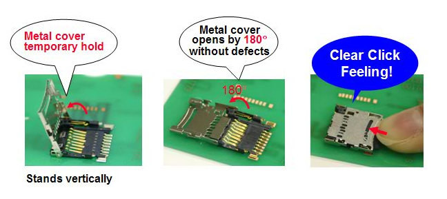
To insert a MicroSD card, slide the connector in the direction of the OPEN-arrow engraved in the metal plate and lift it. Insert the card with the contact area facing down, then fold the connector back in and push carefully in the direction of the LOCK-arrow until it makes a click sound.
External SD Card Connector (External SD)#
The External SD Card Connector provides the option to connect a standard SD card to the iLCD display. demmel products’ DPA-SD-EXT boards is available to interface to the External SD Card Connector.
Speaker Port (Spkr)#
The speaker output may be connected directly to a 4 or 8 Ohm speaker to play sound files.
Jumpers for External Reset Function#
If the external reset function is required, please contact demmel products to learn more about the option to use I/O5 pin as a reset pin instead of a normal I/O5 port.
Maximum Ratings & Power Supply#
Item |
Symbol |
Minimum |
Maximum |
Unit |
|---|---|---|---|---|
Supply Voltage |
VCC |
-0.3 |
5.5 |
V |
Input Voltage |
VIN |
-0.3 |
3.3 |
V |
Operating Temperature 1) |
TOPR |
-20 |
70 |
°C |
Storage Temperature |
TSTR |
-20 |
80 |
°C |
Humidity 2) |
10 |
90 |
%RH |
Notes:
1) Lifetime of backlight LEDs will be decreased for temperatures ≥ 50°C
2) Temp. ≤ 60°C, 90% RH MAX.
3) Temp. ≥ 60°C, absolute humidity shall be less than 90% RH at 60°C
The ground connection to the display should be as good as possible. Especially for iLCDs with projected capacitive touch panel the ground connection to the display and the power supply is crucial for a trouble-free function. If it is not possible or not wanted to connect the power supply with protective earth, this shall be done via a 20 nF capacitor.
Note: The mounting brackets on the iLCD panels are also connected with the PCB’s GND plane.
Quality Standards#
Dust Particles#
The TFT display modules are assembled under clean room conditions. The following table specifies the allowed number and size of particles incorporated.
Dimension (Diameter D) |
Acceptance (Qty N) |
|---|---|
D ≤ 0.25 mm |
Ignored |
0.25 ≤ D ≤ 0.50 |
N ≤ 5 |
D ≥ 0.50 |
0 |
Total |
N ≤ 5 |
Pixel Failures#
For our iLCD Panels we deploy A-grade TFT display modules. We accept a maximum of sub-pixel failures as follows:
Defect Type |
Acceptance (Qty N) |
|---|---|
Bright Dots |
N = 0 |
Dark Dots |
N ≤ 3 |
Total |
N ≤ 3 |
Assembly#
Treatment of the Touch Panel Tail#
The touch panel is connected to the iLCD processor via an FPC tail. It is mounted already on iLCDs with touch functionality. In order to guarantee correct function and to prevent physical damages, please observe the following notes when taking out the iLCD panels from the package and during manufacturing:
Do not exert lateral or shearing forces on the tail. This can happen when fitting the iLCD panel into a housing through a narrow aperture.
Do not crease, twist or pull the tail.
Do not touch the tail conductors.
Treatment of the FFC Tail#
The FFC cable connects the iLCD to the application electronics.
The FFC cable bending radius must be ≥ 3 mm.
Do not exert lateral or shearing forces on the FFC cable.
Do not crease or twist the FFC cable.
iLCD Rear Mount Integration#
One integration method is mounting the iLCD behind a bezel with a rectangular cut out. Rubber or foamed rubber gaskets (cushion) hereby ensure a balancing of tolerances and an environmental sealing. The bezel edge shall be positioned between the LCD Active Area and the View Area. If the bezel edge touches the LCD Active Area, it may press the resistive touch panel unintendedly and cause activation. A gap of approximately 0.5 mm is needed between the bezel and the top electrode. It may cause unexpected activation if the gap is too narrow. There shall be a distance from the panel edge of minimum 1.0 mm for TPC tail protection.